|
半导体 -
半导体制造商压力仪表
Semiconductor -
Pressure instruments for semiconductor manufacturers
全球半导体行业近年来的显着增长预计将持续到 2021 年及以后。主要促成因素包括微电子在电气和电子设备中的应用增加、人工智能、IoT(物联网)以及工业 4.0 计划的扩展。随着这些变化的发生,半导体供应商面临着改善供应以满足需求的挑战——即增加晶体管密度、提高可靠性,当然还有降低生产和采购成本。
Ashcroft 已准备好并愿意帮助半导体制造商应对并克服这一挑战。凭借丰富的行业特定经验,我们拥有知识和技能来帮助开发、设计、制造和测试高质量半导体生产所需的仪器和设备。
我们提供各种压力测量产品,包括采用我们专有的超稳定 CVD 传感技术的变送器,适用于半导体制造应用。我们产品的性能与全球安全认证以及在最关键的半导体应用中的性能相结合。
在半导体工具中,气体面板控制气体流入处理室。压力传感器安装在每个气体棒上的气体面板内部,以监控压力调节器的压力输出。这个位置使他们能够发送信号,以更高的精度、准确度和速度调整系统操作,从而实现更好的整体系统功能。
气体面板
在半导体工具中,气体面板控制气体流入处理室。压力传感器安装在每个气体棒上的气体面板内部,以监控压力调节器的压力输出。这个位置使他们能够发送信号,以更高的精度、准确度和速度调整系统操作,从而实现更好的整体系统功能。
危险气体压力测量
半导体应用中使用的一些气体是有毒的、易燃的,并且对处理它们的人来说是危险的。 这些危险要求许多产品获得 ATEX 和 IECEx 危险场所认证。 日本的 Ashcroft 和 Nagano Keiki Co. Ltd.(我们的母公司)每年生产超过 100,000 个压力变送器和压力表,这些压力变送器和压力表专为在半导体行业应用中安全使用而设计和制造。
氢气压力测量
氢气是超高压气体输送中最常用的载气之一。安全处理氢气需要采取保护措施来降低火灾或爆炸的风险。优选的方法包括本质安全和无火花认证。要记住的一个关键因素是氢脆的影响。压力变送器和压力表的稳定性和可重复性依赖于它们的测量机制(直接与冶金学及其抗脆性相关)。Ashcroft 高纯度变送器和仪表采用高纯度奥氏体 316L 不锈钢,已被证明可以减轻氢脆的影响。
洁净室压力测量
防止污染物渗入洁净室和其他洁净空间所需的压力量是非常具体的。压力太小会导致不需要的颗粒进入该区域,而压力太大会导致空气过度流动并浪费能源。集成到空气处理设备中的压力传感器和仪表必须非常灵敏、准确和可靠。
湿法加工和蚀刻
半导体制造过程涉及将空白硅晶片高度复杂地转变为分立的微电子器件。开发出电路设计和图案,然后将其蚀刻到晶片上。然后可以将晶片分解成单独的电路以用于电子设备。半导体制造不断面临着增加可装入每个晶片的电路数量和密度的挑战。湿法蚀刻使用腐蚀性化学品来进行微细加工。
干蚀刻和等离子灰化
干蚀刻工艺,包括反应离子蚀刻 (RIE),通常用于在硅晶片图案上形成接触孔。它使用活性气体,如碳氟化合物、氧气、氯气和三氯化硼。灰化是一种类似于干法蚀刻的过程,用于去除晶片上的光刻胶(光敏涂层)。等离子灰化使用氧气或氟气,控制这些需要精确压力测量的气体的流速很重要。
化学气相沉积
半导体工业中的化学气相沉积 (CVD) 工艺涉及使用载气(例如氮气或氧气)来稀释有毒气体(例如磷化氢或一氧化二氮)。半导体气体可能易燃、有毒和易爆,因此必须仔细选择具有适当批准用于本质安全或非易燃位置的压力传感器,以解决关键的安全问题。
超纯水/去离子水设施
对于所有污染物类型,超纯水均经过最高纯度处理,而去离子水则去除了所有有机颗粒和溶解气体。晶圆清洗等半导体工艺需要超纯水和去离子水,以防止异物在应用中造成污染,从而对暴露的晶圆表面造成缺陷和损坏。
压力测量在半导体制造中的重要性
如今,半导体制造业务依赖于精确准确地输送超高纯度 (UHP) 气体,这要求纯度水平超过 99.9995% 并严格控制杂散颗粒和水分。鉴于 UHP 供气系统的重要性,用于其分配的测量和控制技术必须提供高精度、高精度的性能,同时保持系统内部的绝对清洁。建筑材料在与超高压气体接触时必须保持惰性,最大限度地减少滞留(死)体积的风险,并防止颗粒脱落和滞留。
虽然对现代半导体的制造至关重要,但超高压气体的毒性和易燃性对处理它们的人的健康和福祉构成了重大风险。出于这个原因,半导体操作中使用的一些设备需要符合泄漏完整性和危险位置规范和标准(例如,ATEX 和 IECEx)以确保用户安全。
Ashcroft 高纯压力测量解决方案
用于半导体制造的 Ashcroft 压力仪表
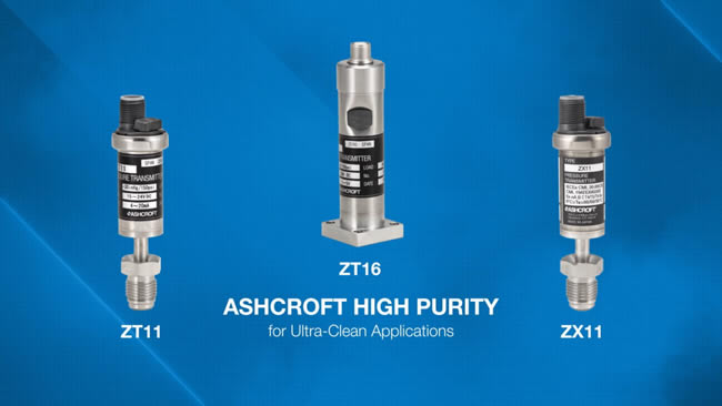
ZT 高纯度变送器和 HPX 高纯度压力表
我们的 ZT/ZX 压力变送器和 HPX 压力表专为半导体应用而设计。这些产品采用电抛光 316L 不锈钢接液部件和 VCR 兼容、模块化和焊接管接头,死体积最小。它们具有紧凑的设计,可在气箱和气体输送系统内容纳更高密度的安装配置。ZX11 包括 ATEC 和 IECEx 危险场所认证。
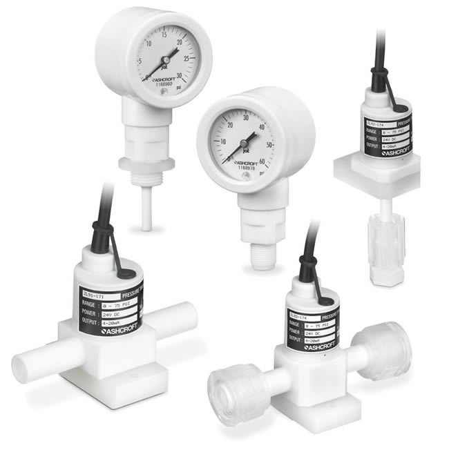
ZL91 压力传感器、ZL92 压力传感器和 HPT - 63 mm 压力表
Ashcroft ZL91 压力传感器由含氟聚合物 (PTFE/PFA) 润湿部件构成,可最大限度地减少金属离子洗脱。其紧凑的设计有助于减少污染并保持过程流体的纯度。该传感器非常适用于超纯水/去离子水设施和设备、半导体清洗设备和湿站应用。
Ashcroft ZL92 压力传感器设计用于需要 PTFE/PFA 接液部件的半导体工艺,以提高在腐蚀性气体和流体(包括氢氟酸或其他腐蚀性酸)中使用的化学兼容性。二级隔离膜片和通风口设计将陶瓷传感元件与腐蚀性气体和液体隔离,从而延长了换能器的使用寿命。该换能器适用于半导体、湿法蚀刻和化学品供应系统的清洁设备。
Ashcroft 63 mm HPT防腐压力表为半导体和电子制造行业的化学品输送系统提供卓越的性能和可靠性。它经过氮气泄漏测试以确保卓越的完整性,而紧凑的设计非常适合有限空间的安装。该仪表由含氟聚合物接液部件制成,使其与使用腐蚀性或非污染流体的工艺兼容。在非污染工艺中,接液部件可防止金属离子洗脱——非常适合超纯水或去离子水工艺。
Ashcroft 硅玻璃传感器技术
用于洁净室和洁净空间的低差压变送器和传感器
我们的许多差压传感器——包括 DXLdp、CXLdp、AXLdp 和 GC30——都集成了Si-Glas ?技术,这有助于它们满足超低差压应用的高度关键的监测和控制需求。压力范围低至 0.05 in H2O (12.5 Pa),可在极低的压力下进行最严格的控制。
我们的 1130 系列压力表设计用于集成到手套箱、晶片处理设备和压差范围低至 0.6 in H2O (150 Pa) 的墙板中。

- HPX高纯压力表 50mm / 63mm high purity pressure gauge
- HPX微型高纯压力表 -28mm HPX Miniatre high purity pressure gauge 28 mm
- ZT11 高纯压力变送器 High purity pressure transmitter
- ZX11 高纯压力变送器 High purity pressure transmitter
- ZT16 高纯压力变送器 High purity pressure transmitter
- HPT - 63毫米压力表 63mm pressure gauge
- ZL91 含氟聚合物压力传感器 FLuoropolymer pressure transducer
- ZL92 含氟聚合物压力传感器 FLuoropolymer pressure transducer
***********************************************************
Semiconductor
Pressure instruments for semiconductor manufacturers
The global semiconductor industry’s significant growth in recent years is expected to continue through 2021 and beyond. Key contributing factors include the increase in the incorporation of microelectronics in electrical and electronic devices, artificial intelligence, IoT (Internet of Things), and the expansion of Industry 4.0 initiatives. As these changes occur, semiconductor suppliers face the challenge of improving supply to meet demand—i.e., increasing transistor density, improving reliability, and, of course, reducing production and purchasing costs.
Ashcroft is ready and willing to help semiconductor manufacturers take on and overcome this challenge. Equipped with extensive industry-specific experience, we have the knowledge and skills to help develop, engineer, manufacture, and test the instruments and equipment necessary for high-quality semiconductor production.
We offer a variety of pressure measurement products—including transmitters with our proprietary ultra-stable CVD sensing technology—suitable for use in semiconductor manufacturing applications. The performance of our products are coupled with global safety approvals and a legacy of performance in the most critical semiconductor applications.
Gas Panels
In semiconductor tools, the gas panel controls the flow of gas into the process chamber. Pressure transducers are installed inside of the gas panel on each of the gas sticks to monitor the pressure output of the pressure regulator. This position enables them to send signals that adjust system operation with greater precision, accuracy, and speed, resulting in better overall system function.
Hazardous Gas Pressure Measurement
Some of the gases used in semiconductor applications are toxic, flammable, and otherwise dangerous to those handling them. These dangers necessitate ATEX and IECEx hazardous location approval for many products. Ashcroft and Nagano Keiki Co. Ltd. of Japan (our parent company) annually produce over 100,000 pressure transmitters and gauges designed and engineered for safe use in semiconductor industry applications.
Hydrogen Pressure Measurement
Hydrogen is one of the most common carrier gases used in UHP gas delivery. Safely handling hydrogen requires the implementation of protective measures that mitigate the risk of fire or explosion. Preferred methods include Intrinsic Safety and Non-Sparking Approvals. One critical factor to keep in mind is the effect of hydrogen embrittlement. The stability and repeatability of pressure transmitters and gauges rely on their measuring mechanisms (directly tied to the metallurgy and their resistance to embrittlement). Ashcroft high-purity transmitters and gauges utilize high-purity austenitic 316L stainless steel, which has been shown to mitigate the effects of hydrogen embrittlement.
Cleanroom Pressure Measurement
The amount of pressure needed to prevent contaminants from infiltrating cleanrooms and other clean spaces is highly specific. Too little pressure results in unwanted particles entering the area, while too much pressure causes excessive air movement and wasted energy. Pressure transducers and gauges integrated into the air handling equipment must be extremely sensitive, accurate, and reliable.
Wet Processing and Etching
The semiconductor manufacturing process involves the highly complex transformation of a blank silicon wafer into discrete microelectronic devices. A circuit design and pattern are developed, which are then etched onto the wafer. The wafers can then be broken into individual circuits to be used in electronic devices. Semiconductor manufacturing is continually challenged to increase the amount and density of the circuitry that can fit into each wafer. Wet etching uses aggressive chemicals to perform microfabrication.
Dry Etching and Plasma Ashing
The process of dry etching, including Reactive Ion Etching (RIE), is commonly used to form contact holes on silicon wafer patterns. It uses reactive gases such as fluorocarbons, oxygen, chlorine and boron trichloride. Ashing is a similar process as dry etching to remove the photoresist (light-sensitive coating) on the wafer. Plasma ashing uses oxygen or fluorine gases, and it is important to control the flow rate of these gases that require accurate pressure measurement.
Chemical Vapor Deposition
The process of Chemical Vapor Deposition (CVD) in the semiconductor industry involves using a carrier gas, such as Nitrogen or Oxygen, to dilute a toxic gas, such as Phosphine or Nitrous Oxide. Semiconductor gases can be flammable, toxic and explosive, so careful selection of a pressure transducer with appropriate approvals for intrinsic safety or non-incendive locations must be made to address critical safety concerns.
Ultrapure/Deionized Water Facilities
Ultrapure water is treated to the highest levels of purity for all contaminant types, and deionized water has all organic particles and dissolved gases removed. Semiconductor processes such as wafer cleaning require ultrapure and deionized water to prevent contamination in the application from foreign particles creating defects and damage to the exposed wafer surfaces.
Importance of Pressure Measurement in Semiconductor Manufacturing
Today, semiconductor manufacturing operations rely on the precise and accurate delivery of ultra-high purity (UHP) gases, which require purity levels to exceed 99.9995% and stringent control over stray particles and moisture. Given the importance of UHP gas supply systems, the measurement and control technologies utilized for their distribution must offer high-precision, high-accuracy performance while maintaining absolute cleanliness inside the system. Construction materials must remain inert when in contact with the UHP gases, minimize the risk of trapped (dead) volume, and prevent particle shedding and entrapment.
While essential to the manufacture of modern semiconductors, the toxicity and flammability of UHP gases pose significant risks to the health and well-being of those handling them. For this reason, some devices used in semiconductor operations are required to comply with leak integrity and hazardous location specifications and standards (e.g., ATEX and IECEx) to assure user safety.
Ashcroft Pressure Instruments for Semiconductor Manufacturing
Ashcroft High-Purity Pressure Measurement Solutions
ZT High-Purity Transmitters and HPX High Purity Pressure Gauges
Our ZT/ZX pressure transmitters and HPX pressure gauges are specially designed for use in semiconductor applications. These products feature electropolished 316L stainless steel wetted parts and VCR-compatible, modular and weld tube fittings with minimal dead volumes. They have compact designs that accommodate higher density mounting configurations inside gas boxes and gas delivery systems. The ZX11 includes ATEC and IECEx hazardous location approvals.
ZL91 Pressure Transducer, ZL92 Pressure Transducer and HPT - 63 mm Pressure Gauge
The Ashcroft ZL91 pressure transducer is constructed with fluoropolymer (PTFE/PFA) wetted parts that minimize metal ion elution. Its compact design helps to reduce contamination and maintain the purity of your process fluid. This transducer is well suited for ultrapure/de-ionized water facilities and equipment, cleaning equipment for semiconductor and wet station applications.
The Ashcroft ZL92 pressure transducer is designed for use in semiconductor processes that require PTFE/PFA wetted parts for improved chemical compatibility for use in corrosive gases and fluids, including Hydrofluoric acid or other aggressive acids. A secondary isolation diaphragm and vent design isolate the ceramic sensing element from corrosive gases and liquids, which extends the life span of the transducer. This transducer works well in cleaning equipment for semiconductor, wet etching and chemical supply systems.
The Ashcroft 63 mm HPT anti-corrosion pressure gauge offers exceptional performance and reliability for chemical delivery systems within the semiconductor and electronic fabrication industries. It’s nitrogen leak tested to ensure superior integrity, while the compact design is ideal for limited space installations. The gauge is made with fluoropolymer wetted parts making it compatible with processes that use corrosive or non-contaminating fluids. In non-contaminating processes, the wetted parts prevent metal ion elution – perfect for ultrapure or deionized water processes.
Ashcroft Si-Glas Sensor Technology
Low Differential Pressure Transmitters and Transducers for Clean Rooms and Clean Spaces
Many of our differential pressure transducers—including DXLdp, CXLdp, AXLdp, and GC30— are integrated with Si-Glas? technology, which helps them accommodate the highly critical monitoring and control needs of ultra-low differential pressure applications. Pressure ranges as low as 0.05 in H2O (12.5 Pa) allow for the tightest control at incredibly low pressures.
Our 1130 Series gauges are designed for incorporation into glove boxes, wafer handling equipment, and wall panels with differential pressure ranges as low as 0.6 in H2O (150 Pa).
Related Products
FAQs
Are there other scales and dial options for the HPX pressure gauges?
Are there other pressure connections available on the ZT/ZX pressure transmitters?
How are the Ashcroft high purity products packaged?
Related Content
Trust in the Ashcroft Experts
At Ashcroft, we are here to help you identify the right pressure instrument for your semiconductor needs. Whether you require gauges, transducers, or transmitters for a standard or cleanroom manufacturing environment, we’ll find the perfect product solution. Trust us with the success and safety of your project.
|